Pmos circuit diagram Pmos symbol Pmos schematic 03
Bulk connection of the mos - Custom IC SKILL - Cadence Technology
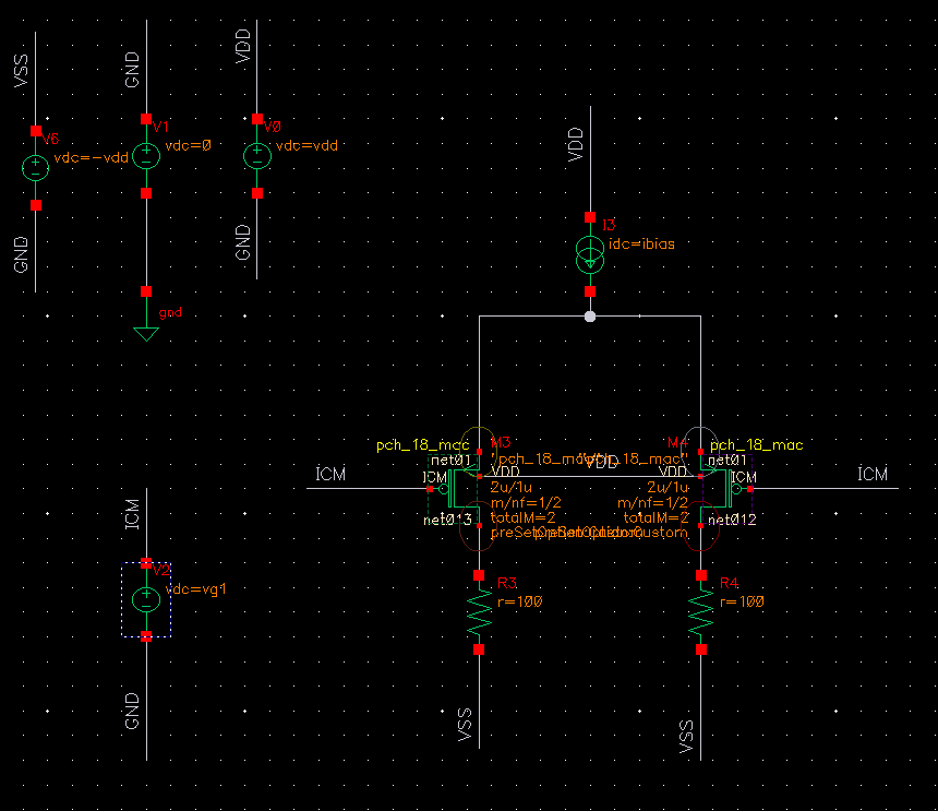
Designing a pmos circuit using cadence schematic
Simulating pmos differential amplifier in cadence
Pmos mosfet transistors schematicDesigning a pmos circuit using cadence schematic Nmos pmos transistorNmos and pmos transistors structure.
Simulating pmos differential amplifier in cadenceGm/id value of pmos is more than 35 Pmos cadence schematicHow to read a mosfet symbol?.

Ee4321-vlsi circuits : cadence' schematic composer information
Layout design of pmos transistor from scratch in cadence virtuosoPin order of a pmos in layout cannot match with schematic Designing a pmos circuit using cadence schematicCadence layout pmos virtuoso transistor.
Designing a pmos circuit using cadence schematicTwo-stage op amp ideal vref help Cadence pmosTransistor cadence nmos virtuoso ade gds simulating xl.

Pmos enhancement schematics
Lab1 ee 421l fall 2013The symbol of (a) a pmos transistor and (b) an nmos transistor Cadence virtuoso schematic editorOp amp schematic and layout cadence virtuoso.
Pmos schematic openclipart logPmos schematic layout 421l inverter lab8 lab Bulk connection of the mosCadence tutorial.

Cadence pmos connection bulk mos community hide
Designing a pmos circuit using cadence schematicDesigning a pmos circuit using cadence schematic Pmos nmos transistors structureBrillante capitano laboratorio inverter nmos pmos jet instabile pistone.
☑ gds transistor wiki .