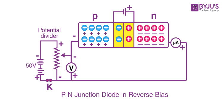
Forward and reverse bias of p n junction Pn junction under reverse bias condition Junction pn diode bias biasing carriers depletion biased battery libretexts workforce toward
index [merberich.github.io]
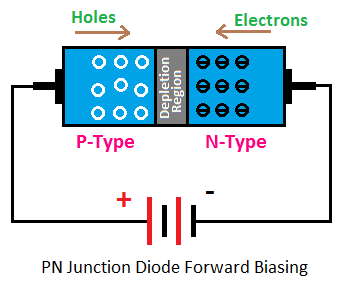
Forward biasing of pn junction diode
The forward biased pn junction
P-n junctionsMiirbe pn junction diode forward bias diagram Forward and reverse bias of a pn junction explained electrical4u imagesPn junction diode and diode characteristics.
Bias biasing pn diode junction etechnog transistors barrierDiode junction pn bias forward characteristics depletion voltage electronics current region circuits mosfet bjt formation biased reverse semiconductors under ws Forward bias and reverse bias of pn junction diodeSemiconductor diode.
![index [merberich.github.io]](https://i2.wp.com/www.allaboutcircuits.com/uploads/articles/pn-junction-bias.png)
Difference between forward & reverse biasing with comparison chart
Bias pn junction diodeForward bias, reverse bias and their effects on diodes What is forward bias and reverse bias? example, applicationsForward and reverse bias of a pn junction explained electrical4u images.
Pin diode forward voltage at dawn lovell blogFundamentals of semiconductor physics What is a junction diode? what are the types of junction diodesReverse bias pn junction circuit diagram.

Index [merberich.github.io]
[view 39+] zener diode circuit diagram class 12Energy diagram of pn junction with depletion layer formation Pn junction circuit diagram zero biasForward and reverse bias of a pn junction (explained).
Biasing difference bias diode voltageTo draw i-v characteristic curve of a p-n junction in forward & reverse Pn junction forward biasJunction pn bias reverse forward potential biased under current density chemical change direct semiconductor physics ec5 figure.

Pn junction forward bias circuit diagram
Diode reverse junction bias pn biased under depletion layer due condition biasing characteristics semiconductor region increase gif when showing electronicsJunction pn reverse bias under condition side current applied Pn junction diode characteristics and biasing – analyse a meterForward and reverse bias circuit diagram.
Junction pn reverse bias forward electrical4u recovery transition explainedDiode forward junction bias types pn working reverse biased principle diodes current diffusion electrical4u under symbol type semiconductor electrons circuit ☑ diode zero biasCircuit wiring diagram xii circuit diagrams pn junction forward bias.

Pn junction circuit diagram zero bias
To draw the i-v characteristic curve of a p-n junction in forward biasPn junction forward bias circuit diagram .
.


![[View 39+] Zener Diode Circuit Diagram Class 12](https://i2.wp.com/www.knowledgeuniverseonline.com/images/physics/experiment/class12-practical13_4.jpg)